- 您现在的位置:买卖IC网 > Sheet目录368 > W9412G6IH-5 (Winbond Electronics)IC DDR-400 SDRAM 128MB 66TSSOPII
W9412G6IH
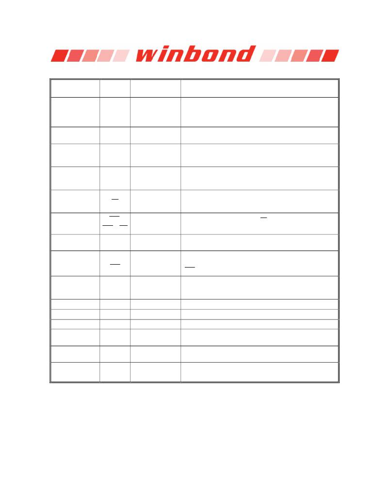
5. PIN DESCRIPTION
PIN NUMBER
28 ? 32,
35 ? 41
26, 27
2, 4, 5, 7, 8, 10,
11, 13, 54, 56, 57,
59, 60, 62, 63, 65
16,51
PIN
NAME
A0 ? A11
BA0, BA1
DQ0 ?
DQ15
LDQS,
UDQS
FUNCTION
Address
Bank Select
Data Input/ Output
Data Strobe
DESCRIPTION
Multiplexed pins for row and column address.
Row address: A0 ? A11.
Column address: A0 ? A8. (A10 is used for Auto-precharge)
Select bank to activate during row address latch time, or
bank to read/write during column address latch time.
The DQ0 – DQ15 input and output data are synchronized
with both edges of DQS.
DQS is Bi-directional signal. DQS is input signal during write
operation and output signal during read operation. It is Edge-
aligned with read data, Center-aligned with write data.
Disable or enable the command decoder. When command
24
23, 22, 21
20, 47
45, 46
CS
RAS ,
CAS , WE
LDM, UDM
CLK ,
CLK
Chip Select
Command Inputs
Write Mask
Differential Clock
Inputs
decoder is disabled, new command is ignored and previous
operation continues.
Command inputs (along with CS ) define the command
being entered.
When DM is asserted “high” in burst write, the input data is
masked. DM is synchronized with both edges of DQS.
All address and control input signals are sampled on the
crossing of the positive edge of CLK and negative edge of
CLK .
CKE controls the clock activation and deactivation. When
44
CKE
Clock Enable
CKE is low, Power Down mode, Suspend mode, or Self
Refresh mode is entered.
49
V REF
Reference Voltage V REF is reference voltage for inputs.
1, 18, 33
34, 48, 66
V DD
V SS
Power (+2.5V)
Ground
Power for logic circuit inside DDR SDRAM.
Ground for logic circuit inside DDR SDRAM.
3, 9, 15, 55, 61
V DDQ
Power (+2.5V) for Separated power from V DD , used for output buffer, to
I/O Buffer improve noise.
6, 12, 52, 58, 64
14, 17, 19, 25,
42, 43, 50, 53
V SSQ
NC
Ground for I/O
Buffer
No Connection
Separated ground from V SS , used for output buffer, to
improve noise.
No connection (NC pin should be connected to GND or
floating)
Publication Release Date: Sep. 16, 2009
-7-
Revision A06
发布紧急采购,3分钟左右您将得到回复。
相关PDF资料
W9412G6JH-5I
IC DDR SDRAM 128MBIT 66TSOPII
W9425G6EH-5
IC DDR-400 SDRAM 256MB 66TSSOPII
W9425G6JH-5I
IC DDR SDRAM 256MBIT 66TSOPII
W947D2HBJX5E
IC LPDDR SDRAM 128MBIT 90VFBGA
W948D2FBJX5E
IC LPDDR SDRAM 256MBIT 90VFBGA
W949D2CBJX5E
IC LPDDR SDRAM 512MBIT 90VFBGA
W971GG6JB25I
IC DDR2 SDRAM 1GBIT 84WBGA
W971GG8JB-25
IC DDR2 SDRAM 1GBIT 60WBGA
相关代理商/技术参数
W9412G6JH
制造商:WINBOND 制造商全称:Winbond 功能描述:2M ? 4 BANKS ? 16 BITS DDR SDRAM
W9412G6JH-4
制造商:Winbond Electronics Corp 功能描述:8*16B DDR1 制造商:Winbond Electronics Corp 功能描述:IC DDR SDRAM 128M 250MHZ 66TSOP
W9412G6JH-5
制造商:Winbond Electronics Corp 功能描述:DRAM Chip DDR SDRAM 128M-Bit 8Mx16 2.5V 66-Pin TSOP 制造商:Winbond Electronics Corp 功能描述:128M BIT DDR1
W9412G6JH-5I
功能描述:IC DDR SDRAM 128MBIT 66TSOPII RoHS:是 类别:集成电路 (IC) >> 存储器 系列:- 标准包装:72 系列:- 格式 - 存储器:RAM 存储器类型:SRAM - 同步 存储容量:4.5M(256K x 18) 速度:133MHz 接口:并联 电源电压:3.135 V ~ 3.465 V 工作温度:0°C ~ 70°C 封装/外壳:100-LQFP 供应商设备封装:100-TQFP(14x20) 包装:托盘
W9412G6JH-5TR
制造商:Winbond Electronics Corp 功能描述:128M DDR SDRAM X16 200MHZ, 65N
W942
制造商:Performance Tool 功能描述:6 Piece Hook and Pick Set 制造商:PERFORMANCE TOOLS 功能描述:6 PC HOOK AND PICK SET
W942508BH
制造商:未知厂家 制造商全称:未知厂家 功能描述:DRAM
W942508CH
制造商:WINBOND 制造商全称:Winbond 功能描述:8M x 4 BANKS x 8 BIT DDR SDRAM
